TRANSMISSION & DISTRIBUTION
Corona shields for thyristor valves at ultra-high voltages
1 May 2009UHVDC operating levels present a particular challenge for the insulation of thyristor valves. AREVA T&D’s R&D teams have carried out electric field stress studies to determine the best profile for the corona shields, built a test object and subjected it to DC and switching impulse tests that validated the theoretical model. The end result after the next phase of development will be a new design of corona shield, suitable for DC applications up to 800 kV.
To deliver over great distances the large quantities of power required to support the rapidly developing economies of countries such as India, China and Brazil, DC transmission schemes at voltages above 500kV and up to ±800kV are now being implemented. Voltages at this level are termed ultra-high votage DC, or UHVDC. These schemes are mainly designed to access remotely located hydroelectric schemes, typically 2000 – 3000 km from the main load centres. Increasing the rating of the converter station equipment from 500kV to 800kV represents a considerable challenge to the equipment designers, mainly related to the dielectric requirements of the equipment exposed to DC stress and in particular to the thyristor valve to ensure that the structure is corona free in normal operation and flashover free under transient over-voltages. Existing corona shield designs suitable for 500kV DC applications would not be suitable for use in 800 kV DC projects.
To achieve a design it is necessary to solve the three-dimensional electrostatic field problem in the vicinity of the corona shields. Because significant reductions in the computation time to create the models for each study could be achieved compared with conventional finite element analysis, Areva’s engineers opted for a boundary element method (BEM) to provide a numerically efficient model of the detailed valve structure.
Thyristor valve design
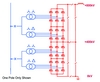
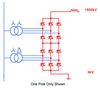
The two designs that can be adopted to achieve an 800kV converter are a single 800kV bridge or two 400 kV bridges connected in series as shown in Figures 1 and 2.
The converter bridges are connected in parallel to increase the power rating. In the diagrams only a single (positive) pole of two identical poles
is shown. In either design the converter transformers, the thyristor valves, and other equipment on the DC bus will experience dielectric stresses up to 800kV. Linear extrapolation from 500kV designs would result in significant over-design of the thyristor valve hall and add unnecessary expense. A thorough investigation of the dielectric design of the thyristor valve was therefore required to ensure that optimal designs for 800kV were arrived at.
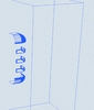
A typical thyristor valve structure (Figure 3) consists of a number of series connected modules, each containing series connected thyristor levels and their grading and damping components. In the design illustrated the zero voltage connection is at the top and the HV connection at the base of the valve structure.
Although the individual thyristor levels experience the same inter-level dielectric stress as a 500kV design, the corona shields are at a higher voltage with respect to earth and must therefore be redesigned, as must the corona shields at the top and bottom of the structure to ensure that the minimum clearance between the lowest shield (at 800kV) and the ground and the walls is achieved. As a single quadri-valve structure could be up to 21m in height, it would be built in two units (0 – 400kV and 400 – 800kV), or four units (0 – 200kV, 200 – 400kV, 400 – 600kV and 600 – 800kV) in the case of a bi-valve design. Consequently the suspension insulator structure and corona shield at the top of the valve also experiences HV, up to 600kV depending on the application. Discharge of energy in stray capacitances into the thyristor during normal switching are controlled by a current limiting reactor installed in the individual valve modules. To re-design the corona shields a major investigation of the electrostatic fields on the valve structure was initiated followed by experimental testing of the new designs.
Basic design
Electrical breakdown occurs when an arc forms between two electrodes, ie a ‘flashover’, complete insulation breakdown usually being preceded by corona discharge. Both effects occur when the localised electrical stress exceeds a threshold value. This stress is dependent on the relative voltage at the electrodes, their separation, the nature of the insulating medium, the geometry of the electrodes and their surface roughness, giving rise to a complex phenomenon that can nonetheless be simplified for certain simple geometries.
The simplest geometry is that of two, large, parallel plate electrodes when the stress is constant and is simply the ratio of the voltage difference to the separation. Given the breakdown stress figure the minimum gap needed to prevent breakdown at any given voltage can be calculated. Design guidance for other geometries tends to follow this example, by relating electrode voltage to electrode separation but even for some simple geometries, this approach has its limitations.
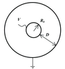
For instance, for two long concentric cylindrical electrodes at a relative voltage V and radial separation D (Figure 4) the stress E at the surface of the inner electrode, radius Rb, is given by:
Even in this simple case, the electric stress is dependent on the curvature of the surface, Rb, as well as on the separation, so achieving a compact and efficient design of valve shielding will be a compromise between shield size and clearances within the valve hall (represented by Rb and D).
For more complex geometries, electrical stress will vary significantly over the surface of the electrode, and be complicated further by multiple electrodes and discontinuities in the electrode surface, eg holes for fixings. To achieve the most efficient design in such cases numerical modelling, and solving the fundamental electromagnetic field equations, is essential.
ES field analysis
The boundary element method was chosen to calculate of the electric field distribution because it is only necessary to discretise the bounding surfaces of the solution domain. In the more widely used finite element analysis the entire volume must be filled with volume elements.
The BEM meshes for the same problem are much easier and quick to build because only the surfaces are to be represented. The field equation describing the voltage distribution is the Laplace equation, where V is the potential difference with respect to earth.
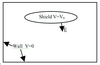
Over the boundary of the problem domain (Figure 5) either the voltage V or its normal derivative must be specified. In the case of the corona shield it is the surface voltage that is known over the shield surface but the normal component of electric field must be calculated. The walls and floor of the valve hall are earthed, providing the outer boundaries of the problem domain.
The BEM is based on surface integral equations. The derivation uses Green’s Second Identity for two scalar functions ? and f:
where O is the solution volume and S is the bounding surface of O. This allows the volume expression for the Laplacian to be expressed as surface integrals in terms of a scalar quantity and its normal derivative, in the electrostatic case the surface voltage and the normal component of surface electric stress.
Applying this leads eventually to the governing BEM equation:
where f is the voltage to be calculated and r, r’ are the geometric positions of points on the surface.
The surfaces of the walls and shield can be discretised using a set of m surface patches. In this case they are triangles over which the voltage is assumed to vary linearly. The normal stress in each element is assumed to have a single value represented at the element centroid. The system of equations for the surface is:
When all the contributions to this equation have been calculated they can be compiled into a set of equations represented by:
where either fj or ?fj/?n is known for each element j. This therefore leads to a system of m equations in m unknowns. Where regions of differing permittivity are present their effects can be included by modifying the coefficient for the normal derivative.
The matrix is solved using the GMRES solver, an iterative technique able to solve large systems of non-symmetric matrices quickly.
Resulting design options
The simple analysis above shows that the radius of curvature of a surface is an important design variable. It rapidly became apparent that, for
800 kV operation, the top and bottom stress shields would have to be formed from a single object having large radius curves, rather than the multiple-plate solution used in the valve illustrated in Figure 3.
It was also clear that the design of the shielding for the individual levels of the valve cannot be considered in isolation from the design of the top and bottom shields, if the most efficient design is being sought.
It was considered that the minimum level of complexity in the prototype shielding system that would adequately represent the full valve structure was a top and bottom shield separated by three levels. Figure 6 illustrates the concept.
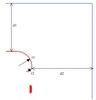
Initially the curved surfaces of the two stress shields were considered to be formed from two radii. The horizontal and vertical clearances were also considered to be adjustable, leading to a problem in four variables (Figure 7). The corners of the shield were formed by ‘sweeping’ through 90° the profile shown, with radius r1.
Boundary element solutions were performed for a number of combinations of the four dimensions, and a series of designs were generated all of which had the same maximum electric field and could be considered equivalently shielding designs.
Trading off the weight and volume of the shield against the clearances (and, ultimately, valve hall size) gives a preferred set of dimensions. External factors, such as the disposition of other components in the valve hall, show the need to have a convenient and reliable means of calculating the electric field distribution for each specific case.
Testing procedure
After creating a numerical model and designing a shielding system verification of the results through prototype testing was essential. Two aspects were concentrated on, the accuracy of the method for modelling structures with high aspect ratios (the shield is made from sheet a few mm thick, but of several square m area) and the level of mesh discretisation needed to produce an accurate solution. To this end, a representative geometry was chosen and a physical prototype was constructed (Figure 6).
The effects of both HVDC and switching impulse (SI) stresses were investigated for a range of test object configurations. The effect of clearance distances as well as the effects of various voltage levels were tried for a range of corona shields types and configurations.
For this, a dummy building consisting of two ground walls 20 m by 20 m to simulate the corner of a valve hall, with a grounded metal frame suspended from a crane to represent the ceiling, was built. Ground and side wall clearances could therefore be independently adjusted.
The HVDC tests consisted of breakdown tests for varying clearances to ground and walls, and corona discharge measurements for set clearances and voltages. Breakdown tests were conducted to investigate both voltage withstand and breakdown levels at determined test object clearances and with various geometries of the shields. A corona camera of the UV detector type was used to accurately locate and correlate measured (surface) corona discharges in various places on the test object.
The SI voltage tests were carried out in accordance with IEC60060-1:1989. U50% breakdown probability was determined using negative and positive switching voltage impulses defined by a 250 µs/2500 µs (±20%/±60%) wave.
Test results
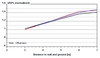
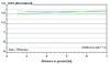
Results for typical stress shield configurations with positive SI voltages are shown in Figures 8 and 9. Figure 8 shows the effect on the breakdown voltage of changing the clearance to the wall and to the ground for three slightly different test conditions. All cases are only for positive voltage switching impulses and the clearance to the wall was the same as the clearance to the ground. The data on the graph have been normalised by the value of the lowest value of U50% achieved.
Doubling the clearance between the lower stress shield and the wall and ground has only increased the voltage withstand by 40%, reflecting the fact that the electrode curvature has an important effect, and it is clear that increasing clearances further only leads to diminishing increases in U50% in line with published data on the behaviour of point-plane and long air gaps.
Figure 9 shows the effect of maintaining the clearance to the wall at 7 m and altering the clearance to the ground.
Again, the voltages have been normalised, and are for positive voltage switching impulses only. The breakdown for this geometry is substantially unaffected by the clearance to the ground. This suggests that the region of highest stress on the lower stress shield is on a near-horizontal surface facing the wall, again showing the importance of the electrode shape.
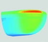
Figure 11 shows the computed distribution of electric stress on the lower stress shield for the model illustrated in Figure 10. In this particular design, the radius of the lower part of the shield (equivalent to dimension r1 in Figure 7) was significantly larger than the radius of the upper part of the shield (dimension r2).
As can be seen, the highest stress in these particular conditions is found on the upper part of the shield (smaller radius) and at the centre of the arc forming the corner. The BEM predicts, therefore, that the highest stress is found at the location of maximum curvature of the surface, although this point is not closest to the earthed walls and floor. It can be seen that stress is not uniformly distributed over the surface of the shield, and changes most rapidly where there is a change in the curvature of the surface.
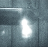
Figure 12 shows a typical example of flashover, one of many breakdowns that occurred between the bottom right hand side of the lower stress shield and ground. Breakdowns occurred in other locations for the same voltage level and configuration, obeying a statistical distribution.
Pre-breakdown investigations were also carried out with HVDC and SI stresses to identify closely the higher stress regions and to look at the propagation of streamers and pre-discharges. For HVDC, the voltage was typically taken beyond partial discharge inception level and to about 50kV lower than known breakdown level to look at streamer activity prior to breakdown. In other cases the voltage was held at the expected breakdown voltage and the time to breakdown measured.
The streamer shown in Figure 13 was very mobile and actually started near the upper lip of the curvature of the lower stress shield corner and progressed downwards to a position similar to the one shown. Full breakdown occurred some 10 seconds after the image was recorded.
Conclusions
Results indicated that the surface profile of the corona shield was a more significant factor than separation from the ground plane in avoiding the inception of corona discharge. Based on the results of the studies, a prototype corona shield was built, which included multiple un-populated thyristor valve modules. This test object was taken to a commercial testing laboratory and subjected to a series of ultra-high DC and switching impulse voltages, confirming the results from the computational study.